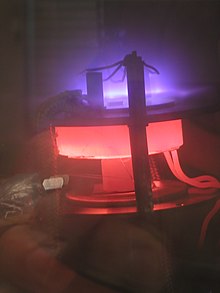
Back ترسيب كيميائي للبخار Arabic CVD Bulgarian Deposició química de vapor Catalan Chemická depozice z plynné fáze Czech CVD Danish Chemische Gasphasenabscheidung German Deposición química de vapor Spanish Keemiline sadestamine aurufaasist Estonian لایهنشانی بخار شیمیایی Persian Kemiallinen kaasufaasipinnoitus Finnish

Chemical vapor deposition (CVD) is a vacuum deposition method used to produce high-quality, and high-performance, solid materials. The process is often used in the semiconductor industry to produce thin films.[1]
In typical CVD, the wafer (substrate) is exposed to one or more volatile precursors, which react and/or decompose on the substrate surface to produce the desired deposit. Frequently, volatile by-products are also produced, which are removed by gas flow through the reaction chamber.
Microfabrication processes widely use CVD to deposit materials in various forms, including: monocrystalline, polycrystalline, amorphous, and epitaxial. These materials include: silicon (dioxide, carbide, nitride, oxynitride), carbon (fiber, nanofibers, nanotubes, diamond and graphene), fluorocarbons, filaments, tungsten, titanium nitride and various high-κ dielectrics.
The term chemical vapour deposition was coined in 1960 by John M. Blocher, Jr. who intended to differentiate chemical from physical vapour deposition (PVD).
- ^ Sadri, Rad (15 January 2021). "Controlled physical properties and growth mechanism of manganese silicide nanorods". Journal of Alloys and Compounds. 851: 156693. doi:10.1016/j.jallcom.2020.156693. S2CID 224922987.