Back Litografia amb feix d'electrons Catalan Elektronová litografie Czech Elektronenstrahllithografie German Elektronkiirlitograafia Estonian طرحنگار الکترونی Persian Elektronisuihkulitografia Finnish Lithographie à faisceau d'électrons French ליטוגרפיית קרן אלקטרונים HE इलेक्ट्रॉन किरण अश्मलेखन Hindi 電子線描画装置 Japanese

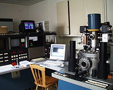
Electron-beam lithography (often abbreviated as e-beam lithography or EBL) is the practice of scanning a focused beam of electrons to draw custom shapes on a surface covered with an electron-sensitive film called a resist (exposing).[1] The electron beam changes the solubility of the resist, enabling selective removal of either the exposed or non-exposed regions of the resist by immersing it in a solvent (developing). The purpose, as with photolithography, is to create very small structures in the resist that can subsequently be transferred to the substrate material, often by etching.
The primary advantage of electron-beam lithography is that it can draw custom patterns (direct-write) with sub-10 nm resolution. This form of maskless lithography has high resolution but low throughput, limiting its usage to photomask fabrication, low-volume production of semiconductor devices, and research and development.
- ^ McCord, M A.; Rooks, M.J. (2000). "2. Electron beam lithography". Microlithography. SPIE Handbook of Microlithography, Micromachining and Microfabrication. Vol. 1. Archived from the original on 2019-08-19. Retrieved 2007-01-04.