Back হ্যাসওয়েল Bengali/Bangla Haswell (microarquitectura) Catalan Haswell Czech Intel-Haswell-Mikroarchitektur German Haswell Spanish Haswell Estonian Intel Haswell Finnish Haswell (microarchitecture) French Haswell Armenian Haswell (hardware) Italian
 | |
| General information | |
|---|---|
| Launched | June 4, 2013 |
| Marketed by | Intel |
| Designed by | Intel |
| Common manufacturer |
|
| CPUID code | 0306C3h |
| Product code |
|
| Performance | |
| Max. CPU clock rate | 800 MHz to 4.4 GHz |
| QPI speeds | 9.6 GT/s |
| DMI speeds | 4 GT/s |
| Cache | |
| L1 cache | 64 KB per core (32 KB instructions + 32 KB data) |
| L2 cache | 256 KB per core |
| L3 cache | 2–45 MB (shared) |
| L4 cache | 128 MB of eDRAM (Iris Pro models only) |
| Architecture and classification | |
| Technology node | 22 nm (Tri-Gate) |
| Microarchitecture | Haswell |
| Instruction set | x86-16, IA-32, x86-64 |
| Extensions | |
| Physical specifications | |
| Cores |
|
| GPUs |
|
| Sockets |
|
| Products, models, variants | |
| Models |
|
| Brand name |
|
| History | |
| Predecessors | Sandy Bridge (tock) Ivy Bridge (tick) |
| Successors | Broadwell (tick/process) Skylake (tock) |
| Support status | |
| Unsupported | |
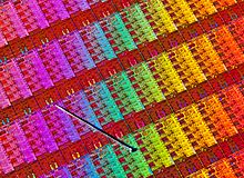
Haswell is the codename for a processor microarchitecture developed by Intel as the "fourth-generation core" successor to the Ivy Bridge (which is a die shrink/tick of the Sandy Bridge microarchitecture).[1] Intel officially announced CPUs based on this microarchitecture on June 4, 2013, at Computex Taipei 2013,[2] while a working Haswell chip was demonstrated at the 2011 Intel Developer Forum.[3] Haswell was the last generation of Intel processor to have socketed processors on mobile. With Haswell, which uses a 22 nm process,[4] Intel also introduced low-power processors designed for convertible or "hybrid" ultrabooks, designated by the "U" suffix. Haswell began shipping to manufacturers and OEMs in mid-2013, with its desktop chips officially launched in September 2013.
Haswell CPUs are used in conjunction with the Intel 8 Series chipsets, 9 Series chipsets, and C220 series chipsets.
At least one Haswell-based processor was still being sold in 2022 — the Pentium G3420.[5][6] Windows 7 through Windows 10 were released for the Haswell microarchitecture.
- ^ "Intel Developer Forum". Intel.com. Intel. Retrieved 2012-01-04.
- ^ Moorhead, Patrick (4 June 2013). "Intel's Newest Core Processors: All About Graphics And Low Power". Forbes.
- ^ Crothers, Brooke (2011-09-14). "Haswell chip completes Ultrabook 'revolution'". News.cnet.com. Retrieved 2012-01-04.
- ^ "IDF 2008 Shanghai : Compte-rendu Processeur : de Nehalem à Haswell". x86 Secret. Archived from the original on 2011-07-18. Retrieved 2012-01-04.
- ^ "Haswell is back: Intel reverses decision to discontinue 22nm Pentium CPUs". TechSpot. 7 December 2019. Retrieved 2021-04-12.
- ^ Shilov, Anton. "Intel Un-Discontinues Pentium G3420 'Haswell' CPU". www.anandtech.com. Retrieved 2021-04-12.